数字系统与微处理器-常考知识点
本文最后更新于 2025年6月4日 晚上
Knowledge points of Digital Systems and Microprocessors
Made for the final test of Brunel University 2020 EE1655: Digital Systems and Microprocessors
Lecturer: Dr.Zhengwen Huang(黄正文)/Dr. Guoquan Li(李国权)
*: appeared in all 3-year final tests
(Given table): the reference is given in the test paper
Basic knowledge of binary code and Boolean algebra
Conversion between Dec BCD, Hex and Binary*
X-based to Dec:
\[∑_{k=0}^na \times x^k\] ec to X-based:
Successive division
m-in-n/m-out-of-n/m-of-n codes
N stands for total number bits
M stands for m bits must be set to 1
If the number of 1 in a data package is not equal to m, error happens
Parity code
The number of 1 in a line is consistently to be even/odd. 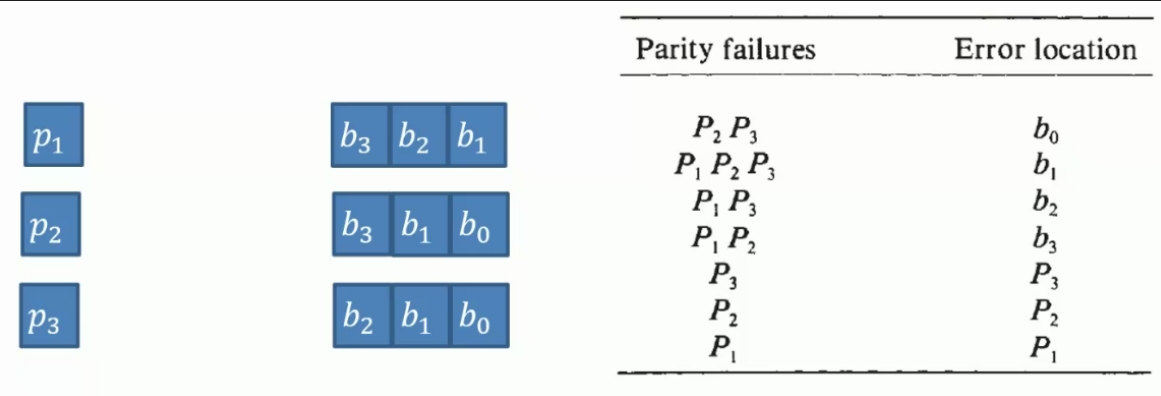
Truth table equivalence*
If two Boolean functions share the same truth table, they are equal.
Combinational logic
1st and 2nd canonical form*
1st canonical form: (.)+(.)
the result of Kmap: 0: F, 1:T
2nd canonical form: (+).(+)
the result of Kmap: 0:T, 1:F
Relation: \(F_{1st}+F_{2nd}=1\)
They share the same Kmap.
Conversion between NAND NOR version*
1st canonical form to NAND version:
\[A.B+C.D=\overline{(\overline{A}.\overline{B}).(\overline{C}.\overline{D})}\]
2nd canonical form to NOR version:
\[(A+B).(C+D)=\overline{\overline{A+B}+\overline{C+D}}\]
Cellular Logic
Recursive function
Sequential logic
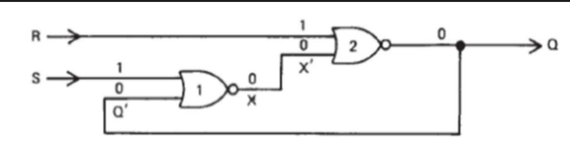
Structure of SRFF
Characteristics of TFF and DFF*
TFF:
Structure:
Asynchronous TFF: J=K=1 CLK=T
Synchronous TFF: J=K=T CLK=CLK
Functionality:
T=0 keep the state
T=1 change the state

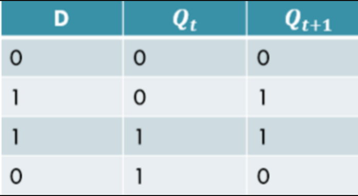
DFF: Structure:
\(J=D\) \(K=\overline{D}\)
Functionality:
whenever the current state is, the next state will be D.
Feedback Shift Register*
Method: move the head bits to the tail, with possible options.
Counter
Counter is used to generate a sequence.
Circuit design (Transition diagram, P/N state table, Transition table, K-maps)*
Transition diagram:
Set A=00 B=01 C=11 D=10
Input is IA/B/C/D, list the transition table.
Digital System
Multiplexer and design*
Simplify some variables in Boolean function, the simplified variables will be used for encoder part.
The meaning of n to 1: the number of control bits will be 2^k=n
Memory and how to determine its size
The memory is determined by the number of logic gates which connected to R/W line.
The size of memory= number of gates x number of layers bits.

Introduction of PIC
The basic information of PIC16F876A*, including:
The size of Program memory/Code memory is 8k bits, Data memory is 13k bits, Program counter(PCL) is 13k bits and located in data memory.
The maximum level of stacks is 8, with 13 bits width.
Number of Pins is 40 (DIP40).
Harvard Architecture.
There are 35 instructions for PIC16F876A.
The location and functionality of SFRs:
- W register: outside of program memory, the data transition station
- STATUS register: Program memory, determine which bank in program memory will be used
Functionality of some assembly language instructions (Given the table)*, including:
- BSF: set the file register to be 1
- BCF: clear the file register to be 0
- NOP: do nothing but create a 1 bit delay
- BTFSC: bit check, if file register is cleared, then skip the following line
- BTFSS: bit check, if file register is set, then skip the following line
Conversion between Two’s complement and Dec*
Positive Dec number: convert to binary number, then keep it.
Negative Dec number: remove “-”,convert to binary number, do complement on the number, then +1.
Conversion between assembly language instructions and machine code* (Give the table)
Structure of machine code:
- operation code
- destination
- file address
4 kinds of characters of instruction’s 14-bit Opcoder:
- K literal
- X don’t care (default to be 0)
- D W register (1 for W register to File register, 0 for File register to W register)
- F file register’s address
- b bit address within an 8-bit file register
Subroutine’s explanation by explaining instructions like CALL, GOTO and RETURN and time consumption* Time/Cycle consumption: Normal execution costs 1 us, GOTO and RETURN instruction costs 2us.
Track the value of W register
Output Devices*
7-Segments:
Port A: which 7-segments will be lighten
Port B: display the number (0:light, 1:dark)Keypad:
Switch Bounce: There should be a delay to wait the time in order to let the key bounce (about10-3s) be finished, or may cause the hazard.
ADC
Precession and LSB: \(LSB=\frac{Range}{2^k}\) , k is the number of bits
Quantity error: ⁺-0.5 LSB