5. 组合逻辑2:用数字逻辑电路实现[英]
本文最后更新于 2025年6月4日 晚上
Combinational Logic 2: Implementation using Digital Circuit
Logical transformation
To deal with the lack/limit of circuit components, the transformation are introduced.
In implementation of circuits, an implementation of 2-input NAND/NOR gate requires 2 transistors (晶体管), however, a 2-input AND/OR gate requires 4 transistors. To save the cost, NAND logic and NOR logic are introduced to transform the 1st/2nd canonical form into a NAND/NOR only used circuit.
NAND logic and 1st canonical form
AND to NAND
\[F=A.B=\overline{\overline{A.B}}\]
OR to NAND
\[\overline{A.B}=\overline{A}+\overline{B}\] \[A+B=\overline{\overline{A}+\overline{B}}\] The AND and OR gates can be replaced with their NAND equivalents for the 1st canonical form giving.
NOR logic and 2st canonical form
The NOR can be obtained from the minimal 2nd canonical by replacing AND and OR gate.
AND to NOR
\[A.B=\overline{\overline{A}+\overline{B}}\]
OR to NOR
\[A+B=\overline{\overline{A}.\overline{B}}=\overline{\overline{A+B}}\]
Don’t care condition(无效项)
The binary input combinations may never occur although they exist. For example: in BCD(0-9) coding 1010(10) to 1111(15) are never used.
Example: Seven Segment Display
To represent numbers, corresponding segments will be lighten.
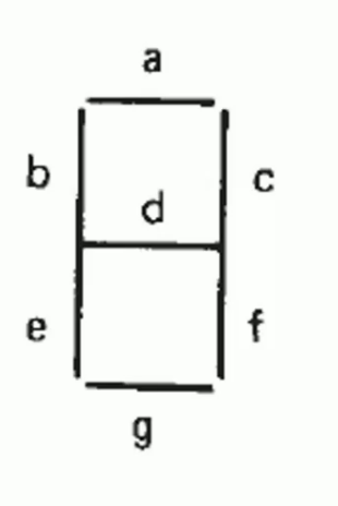
Example:
- 0->a b e g c f
- 2->a c d e g
- 7->a c f
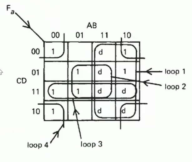
To control segment a, we will design a system. When number=0,2,3,5,7,8,9 \(F_a=1\).
In binary we need 4 bits to present the numbers 0-9, but 10-15 will be never used.
All possibilities are listed using Kmap.
The circuit adding don’t care condition is not equal to the origin one, but the difference is omitted, so they are still equivalent.
Harzard and Risk(竞争冒险)
Practical electronic logic circuits are not ideal devices. They require a finite time to operate and consequently introduce delays into the propagation of information.
- no more than a few \(10^{-6}\)s.
- for very high speed logic, may be of the order of \(10^{-9}\)s
- they may invalidate the laws of Boolean algebra and cause errors or hazard the logic state.
The generation of harzards are caused by when a “1” and a “0” inputted into a logical gate within a short time. (i.e., like \(F=A\overline{A}\) or \(F=A+\overline{A}\))
Elimination of Hazards
Solution 1 : Wait and consider the valid output
If the maximum number of gates in any propagation path is \(𝑛\) and the delay of each gate is \(𝑑𝑡\), the output of a combinational logic circuit will always be valid at time \(T\), thus:
\[ 𝑇 > 𝑛 × 𝑑𝑡\]
Solution 2: Delaying gate arrangements
To replace the gates with long logical equivalent gates combinations.
- have no effect on the value of the data.
- will present a delay.

Solution 3: K-maps
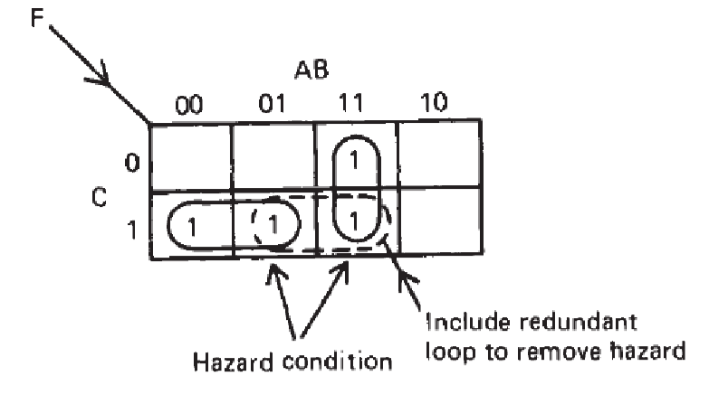
- A hazard will always occur when switching between adjacent cells on a K-map that are unlooped.
- The hazard can be removed by looping the adjacent cells even if it involves introducing an otherwise redundant term into the function.
- A K-map can be used to detect and eliminate all hazards arising from the switching of any one variable.
Cellular Logic
In cellular logic circuit, the logic functions can be transformed into cells with external I/O and internal I/O.
- \(I\) input of a cell
- \(Z\) output of a cell
- \(Q\) internal outputs of a cell and connects other cells.
Example: 2bits adder \[S_2S_1S_0=A_1A_0+B_1B_0\] By listing the truth table and draw Kmaps, the presentations are:
\[S_2=A_1B_1+A_0B_1B_0\] \[S_1=A_1\overline{B_1}\overline{B_0}+A_1\overline{A_0}B_1+\overline{A_1}\overline{A_0}B_1+\overline{A_1}B_1B_0+\overline{A_1}A_0\overline{B_1}B_0+A_1A_0B_1B_0\] \[S_0=A_0\overline{B_0}+\overline{A_0}B_0\]
For a two-bit adder, the internal relationship are very complex, in this case, the whole circuit can be regarded as a black box when a two-bit adder is used. Only inputs and outputs are users cares about.
But above logical presentations are not so universal when confronting with inputs with more bits. In this way, a one-bit adder can be regarded as a universal cell as:
For an adder cell:
- \(A\) \(B\) are the external inputs.
- \(S\) are the external outputs.
- \(C\) for carry-in and carry-out is the increment I/O.
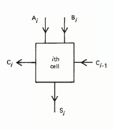
By adding more the same cells, the adder can support input with more bits:
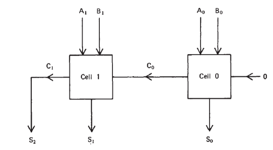
Therefore, a logic relationship in this single cellular is:
\[C_i=A_iB_i+A_iC_{i-1}+B_iC_{i-1}\] \[S_i=\overline{A_i}\overline{B_i}C_{i-1}+A_i\overline{B_i}\overline{C_{i-1}}+\overline{A_i}B_i\overline{C_{i-1}}\]