7. 时序逻辑2:时序逻辑电路的设计[英]
本文最后更新于 2025年6月4日 晚上
Sequential Logic 2: Circuit Design
Next State Feedback Logic
The sequenctial logic circuit operating the external inputs and internal state, feedback to form internal inputs, which is called next state feedback logic (次态反馈逻辑).
In next state feedback logic, parameter of a sequential circuit are:
- \(I\) input data
- \(Z\) output data
- \(Q\) internal data sets(also called states)
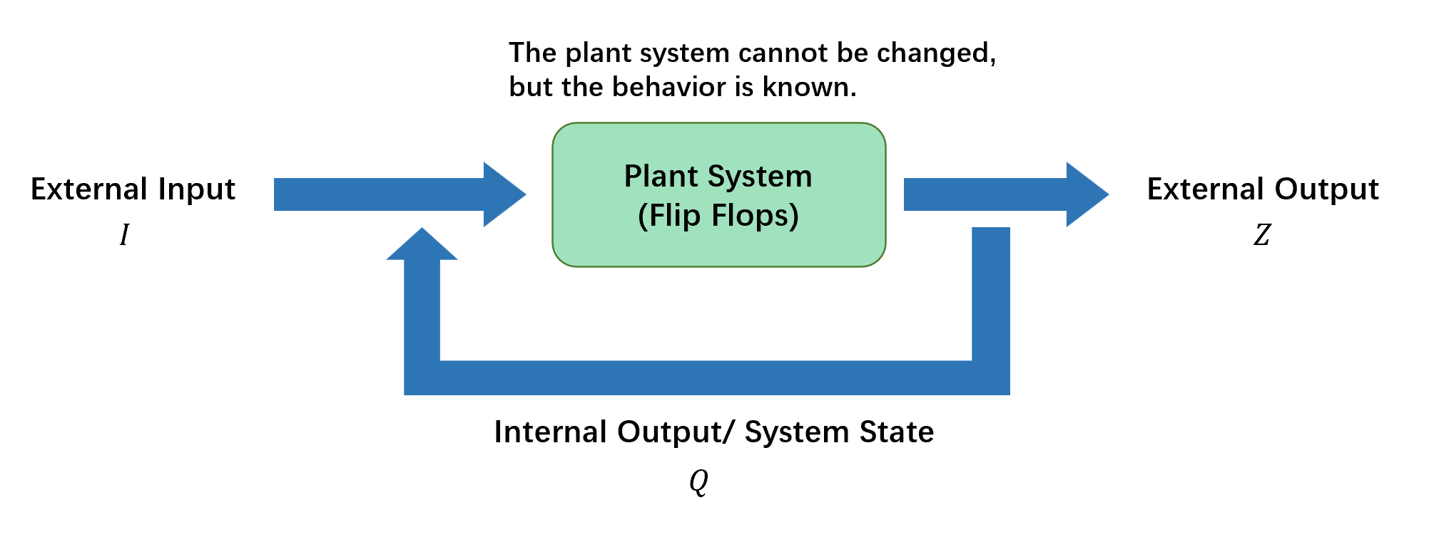
The flip-flops themselves are to produce the changes from current state to another state, they are a kind of next state feedback logic.
The designer of the next state logic has to be able to identify the internal states of the plant system and then design hardware to generate them.
Thus, the design of sequential logic is to utilize the behaviour of plant system and modify the output end or the input end of the flip-flops to make flip-flops produce a desired overall system behaviour.
In addtion, it can be found that, in real system design the only contribution of next state logic is to produce a motivation of state changing.
Output Logic
In this design concept, the modicifactions will be implemented onto the output end of next state feedback logic to produce a desired system output.
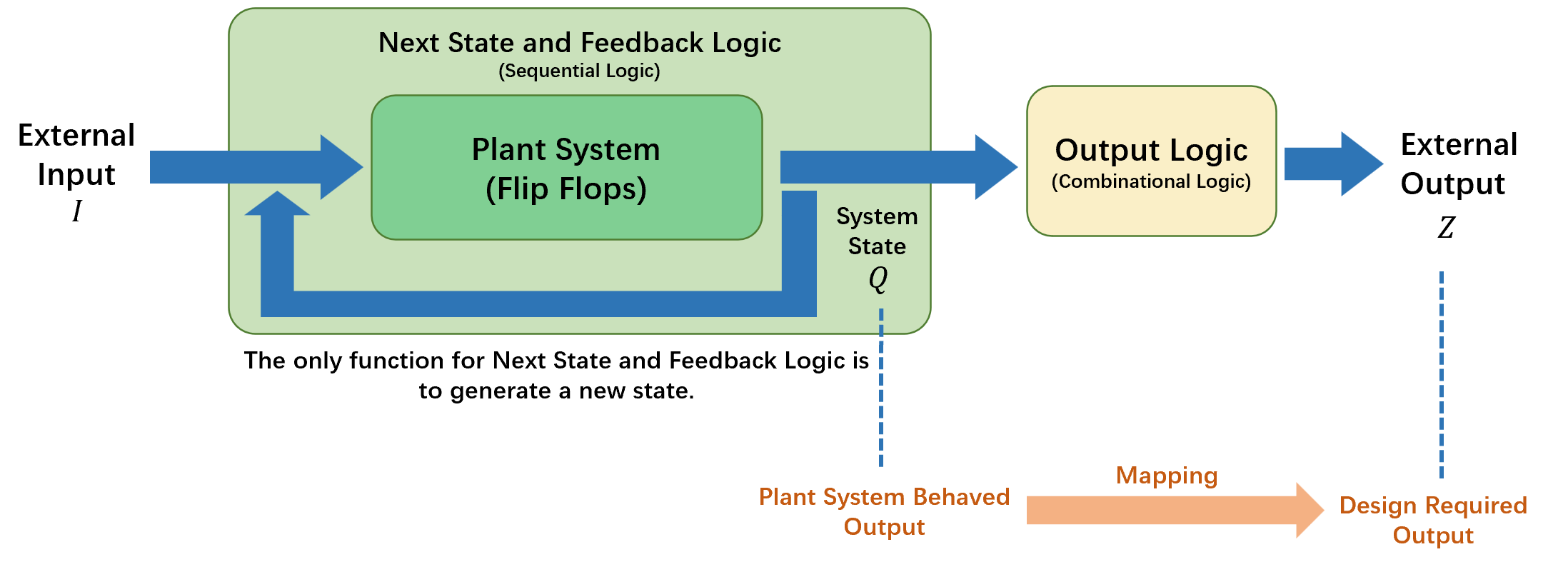
The overall system is combined as:
- Inputs of the output logic are external input \(I\) and the state \(Q\).
- The combinational logic circuit part to generate output \(Z\).
Besides, Automatic logic is a kind of logic which only has internal inputs and outputs.
Implementation
Implement such a kind of logic requires:
- Combinational logic with feedback
- Standard flip-flops
- Memory
The implementation steps:
- identify the standared flip flops.
- drive k-map between desired ouput and the output of next-state feedback logic circuit.
Example: A 3-bit counter count in Gray Code
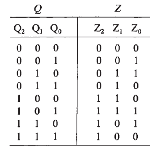
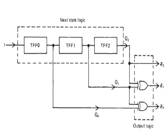
For 3-bit counter, it can be regareded as a next-state feedback logic to produce the state changing. The relationship between output of counter \(Q\) and desired output \(Z\) is:
Based on this truth table, the K-map is:
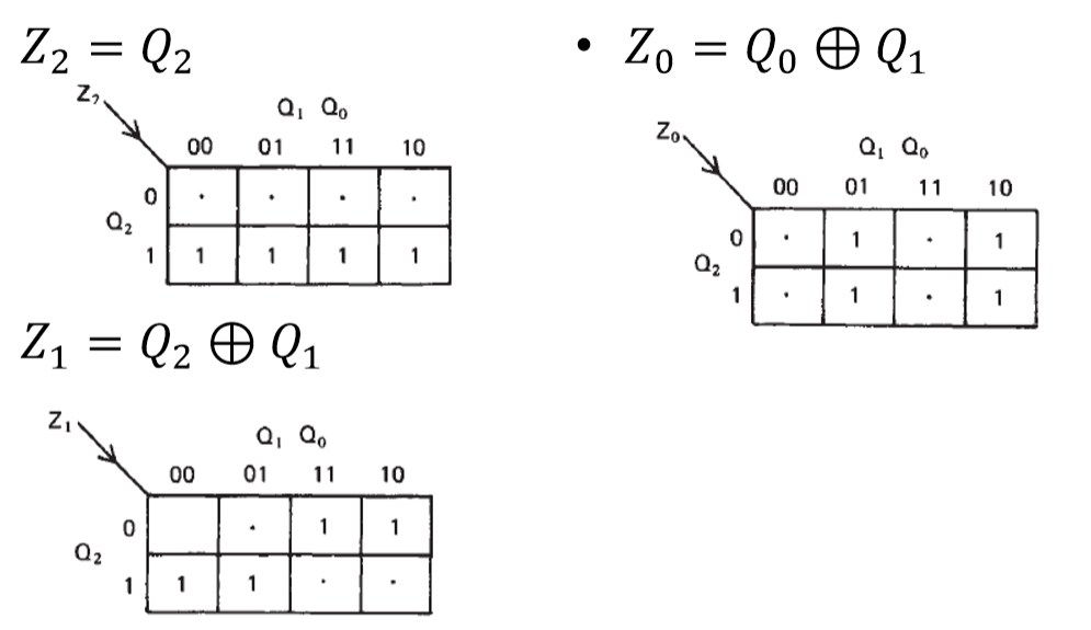
Thus, the circuit for a Gray Code counter using output logic is:
Driving Logic
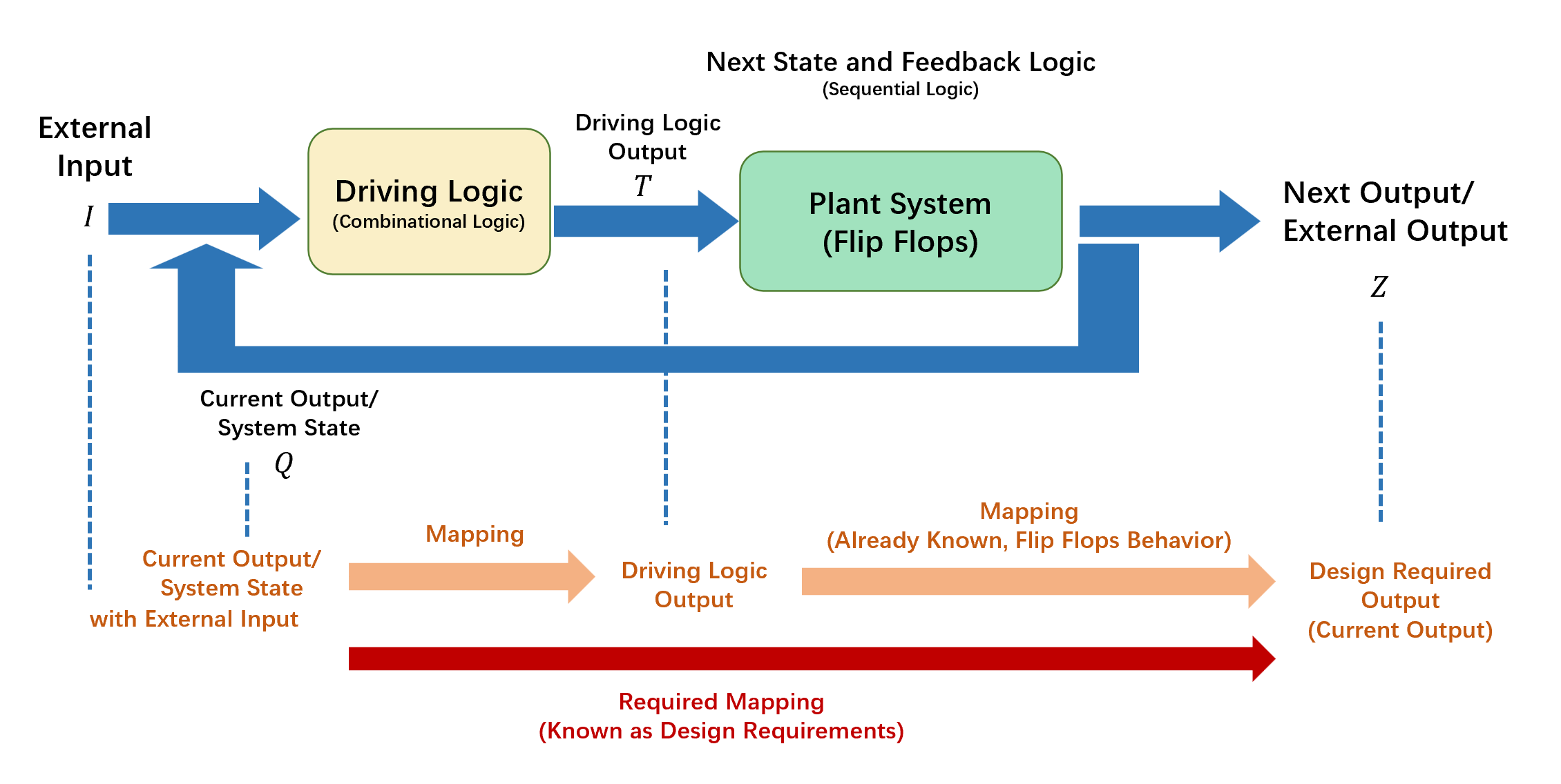
Another design method to make the fixed system plant to produce the desired output is to modify the system plant’s input end.
Thus, in driving logic, the modification of system is on the input end of system plant to change the flip flops’ input to produce the desired output.
Present/Next Table
In this way of design, the design objective is to find out the mapping between prvious output \(Q\) (with external input \(I\)) and drving logic output \(T\) which can further drive the mapping between prvious output \(Q\) (with external input \(I\) ) and external output \(Z\).
To achieve this objective, the driving logic output for every possible state need to be identified firstly.
This output can be obtained by observing the change between the previous output \(Q\) and Next Output \(Z\). Present/Next Table (状态转换表) is a tool help with listing all the previours output and Next Output.
Example: A typical Present/Next Table of 3-bit counter is like this:
| Current Output \(Q\) |
Next Output \(Z\) |
|---|---|
| 000 | 001 |
| 001 | 010 |
| 010 | 011 |
| 011 | 100 |
| 100 | 101 |
| 101 | 110 |
| 110 | 111 |
| 111 | 000 |
It is highly recommended to add another colounm to specify each driving logic output \(T\).
Suppose this 3-bit counter is realized by using 3 TFFs:
| Present Output \(Q\) |
Next Output \(Z\) |
Driving Logic Output \(T\) |
|---|---|---|
| 000 | 001 | 001 |
| 001 | 010 | 011 |
| 010 | 011 | 001 |
| … | … | … |
Implementation
Autonomous Sequential Circuits
This kind of circuits does not have any external input \(I\), the synchronous system will need a clock.
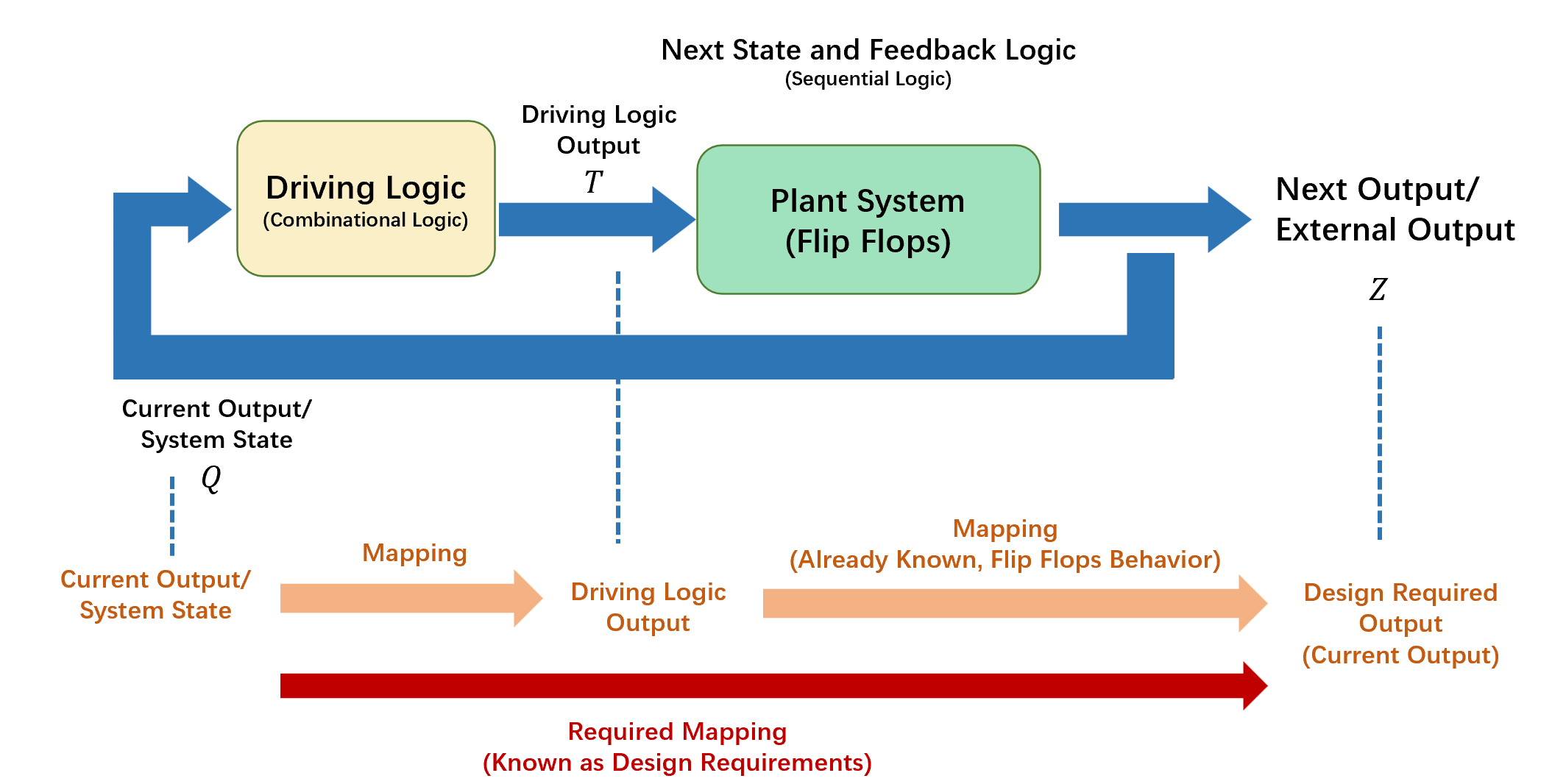
when \(T\) is determined, the combinational logic between \(Q\) and \(Z\) can be identified by driving kmaps.
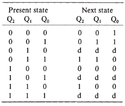
Example: 3 bits Code Generator
Providing the code cycle at one word per clock pulse:
\[000 → 001 → 011 → 110 → 100\]
According to the requirements, the P/N table is shown as:
Suppose JKFFs are used to build the system plant:
| \(J\) | \(K\) | \(Q_t→Q_{t+1}\) |
|---|---|---|
| 0 | d | 0→0 |
| 1 | d | 0→1 |
| d | 0 | 1→1 |
| d | 1 | 1→0 |
Thus, the \(J\)s and \(K\)s for each column can be determined.
For example, for \(001→ 011\),for \(Q_0\) (the JKFF corresponding to the first bit): \(1->1\) compared with JKFF’s behaviour table, it can be obtained that: \(J_0=d\) and \(K_0=0\).
Thus, kmaps of \(J_0\) and \(K_0\) can be obtained:

(red circles are the examples mentioned above)
Finally, it can get:
\(J_1=Q_2\), \(J_2=Q_1\), \(K_1=\overline{Q_2}\) \(K_2=\overline{Q_1}\)
Sequential Circuits with External Input
In this kind of circuit, there is an external input \(I\) which controls the output.
For example, \(I\) can be used as a switch signal: when \(I=0\), system keeps the current behaviour, when \(I=1\), system jump to other output. Or \(I\) can be used as a mark of counter: when \(I=0\), Next Output = Current Output +1, when \(I=1\), Next Output = Current Output - 1.
Thus, when driving the P/N table, the value of external input \(I\) should be considered.
Example: A Present/Next Table of \(I\)-controlled Up-down 3-bit counter is like this:
| Current Output \(Q\) |
Next Output \(Z\) \(I=0\) (up) |
Next Output \(Z\) \(I=1\) (down) |
|---|---|---|
| 000 | 001 | 111 |
| 001 | 010 | 000 |
| 010 | 011 | 001 |
| 011 | 100 | 010 |
| 100 | 101 | 011 |
| 101 | 110 | 100 |
| 110 | 111 | 101 |
| 111 | 000 | 110 |
The next step is to get the input of flip-flops for each \(I\) and each \(Q\).
Example: Suppose a 3-bit up-down counter is realized by using 3 TFFs:
| Current Output \(Q\) |
Next Output \(Z\) \(I=0\) (up) |
Driving Logic Output \(T\) \(I=0\) (up) |
Next Output \(Z\) \(I=1\) (down) |
Driving Logic Output \(T\) \(I=1\) (down) |
|---|---|---|---|---|
| 000 | 001 | 001 | 111 | 111 |
| 001 | 010 | 011 | 000 | 001 |
| 010 | 011 | 001 | 001 | 011 |
| … | … | … | … | … |
when \(T\) is determined, the combinational logic between \(IQ\) and \(Z\) can be identified by driving kmaps.
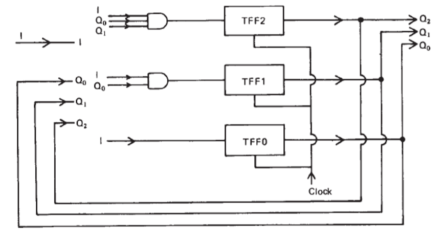
Example:A switch controlled 3-bit Timer
In this timer, the exteranl input \(I\) is used as a switch, when \(I=0\), the counting procedure is paused; when \(I=1\), the counting procedure is continued.
According to the requirements, the P/N table is shown as:
| Current Output \(Q\) |
Next Output \(Z\) \(I=0\) (switch off) |
Next Output \(Z\) \(I=1\) (switch on) |
|---|---|---|
| 000 | 000 | 001 |
| 001 | 001 | 010 |
| 010 | 010 | 011 |
| 011 | 011 | 100 |
| 100 | 100 | 101 |
| 101 | 101 | 110 |
| 110 | 110 | 111 |
| 111 | 111 | 000 |
TFF can provide the state change( just depend on real situation, JKFF is OK).
Synchronous TFFs will be used for this circuit.
Kmaps are:

The diagram is:
Cellular Sequentail Logic
A large number of input variables, the canonical forms become increasingly complex and unwieldy. Any minor change(e.g. add one more variable) in the specification of the system often leads to a major redesign of the circuit.
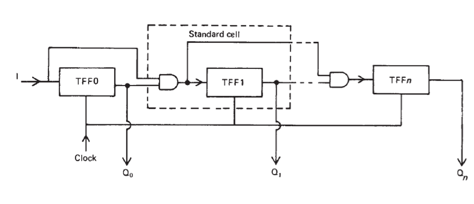
To solve this problem, the cellular can be designed, in cellular diagram, the repeat parts are condensed into Standard Cell, they enable the resolution in the logic system to be increased without requiring a total redesign of the system.
Example: n-bit timer
Using TFFs to complete this task:
In cellular form:
\[T_0=I\] \[T_1=I.Q_0\] \[T_2=T_1.Q_1\] \[…\] \[T_n=T_{n-1}.Q_{n-1}\] Its Cellular diagram is:
State Transition Diagram
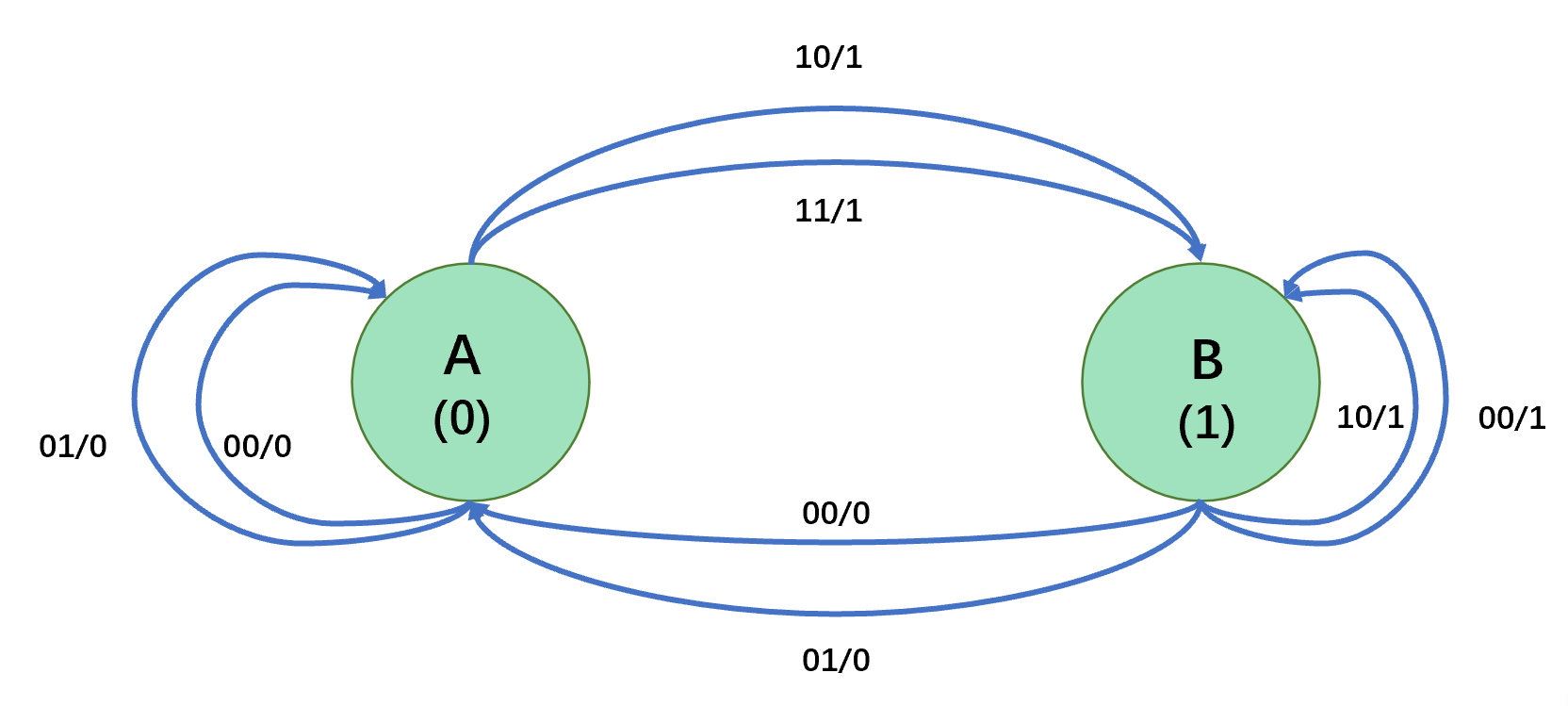
state transistion diagram(状态转换图)is a graphical representation of a sequential system.
The state transition diagrams can be easily transferred to the N/P tables.
It contains two basic elements:
- Nodes: represent the internal states.
- Flow lines: connect nodes labelled with the inputs causing the state transition and the resulting output.
Meanwhile, every flow starts from and terminates in a node.
Besides, each flow line will have a corresponding comment in the form like “input value/output value”.
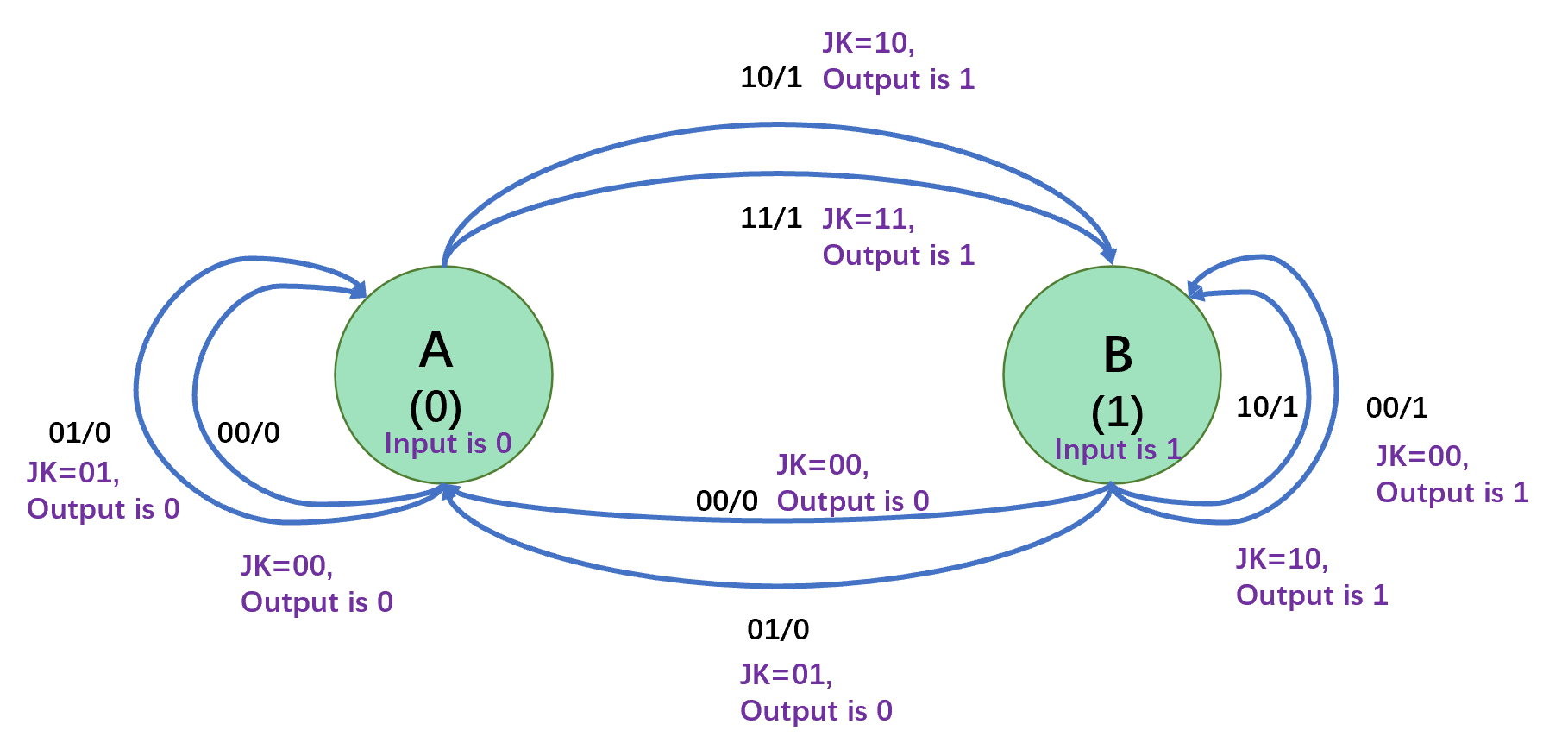
Example: a state transistion diagram of JKFF is shwon as:
The annotations are shown as follows:
Example: Sequence detector(序列检测器) If the input sequence is \(101\), then the output is \(001\). Otherwise, the output is \(000\).
Its state transition diagram is:
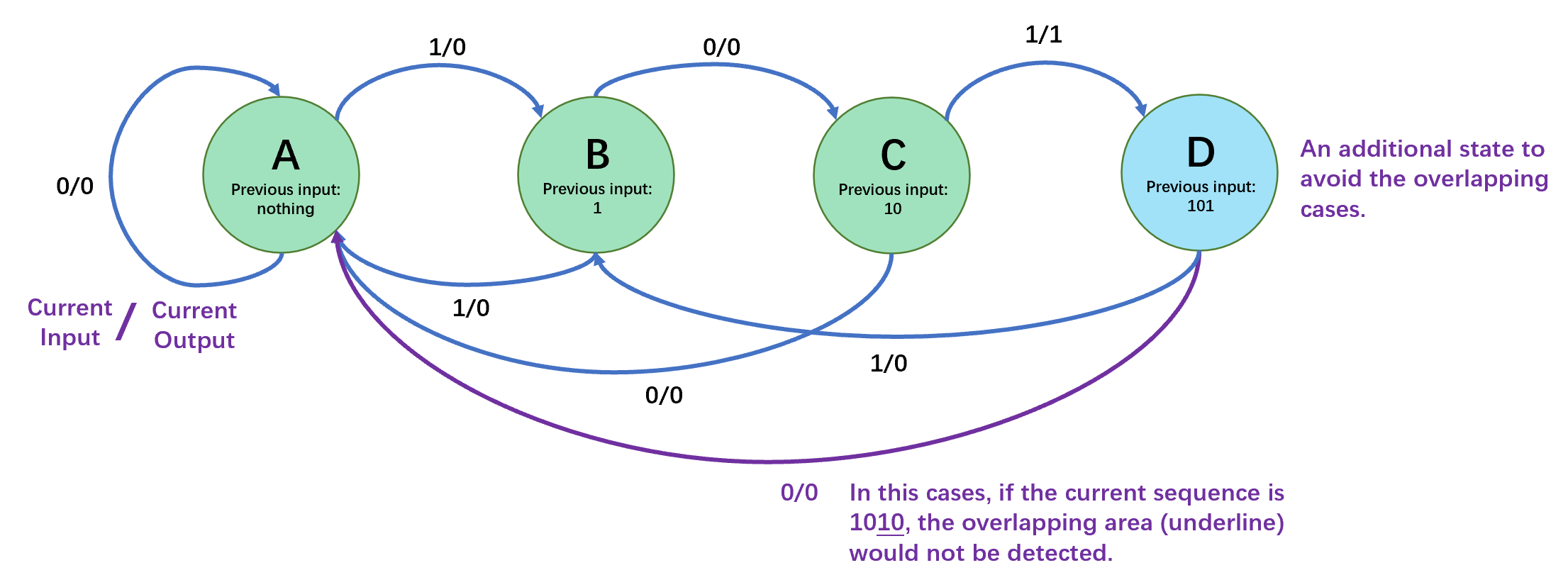
• Node A
- Input \(I = 0\) , stay in \(A\)
- Input \(I = 1\), go to \(B\).
- Output both \(0\).
• Node B
- Input \(I = 1\), stay in \(B\)
- Input \(I = 0\), go to \(C\)
- Output both \(0\).
• Node C
- Input \(I=0\) go to \(A\) output \(0\)
- Input \(I=1\) go to \(D\) output \(1\)
• Node D
(Here State \(D\) is used to avoid the overlaping cases like 1010)
- Input \(I=1\) go to \(B\) output \(0\)
- Input \(I=0\) go to \(A\) output \(0\)
It can be transferred to P/N table containing nodes.
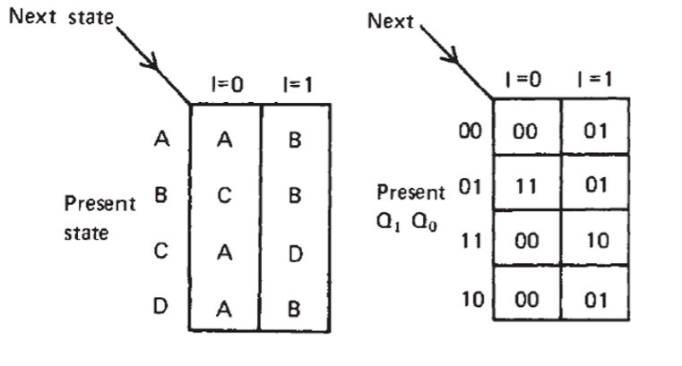
Where states are ranked with gray code: \(A = 00\), \(B = 01\), \(C = 11\) and \(D = 10\) Meanwhile, Two JKFFs will be needed.
Acorrding to the P/N table, the \(J\)s and \(K\)s in different present states can be obtained according to its characteristics.
Thus, the Kmaps between \(T\) and \(Q\) can be constructed as:
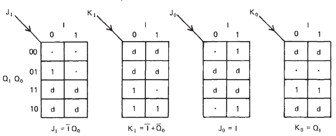
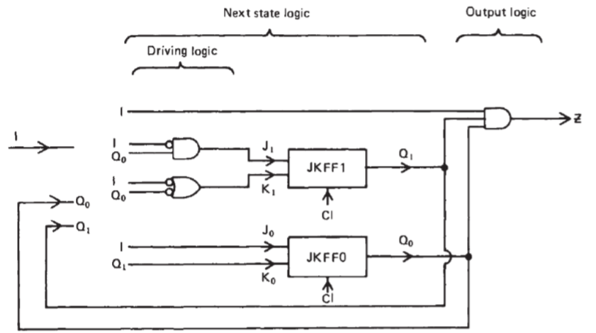
Final circuit is:
Minimization
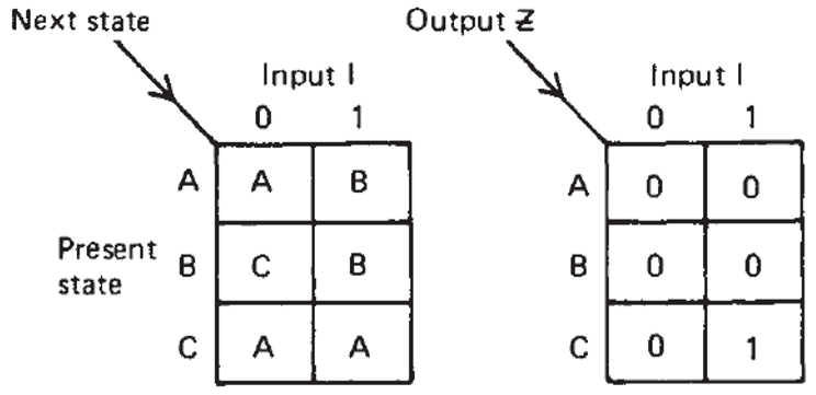
In P/N State table, if two rows are the same, the one of the states can be reduced.
Example:
In previous P/N table:

row A and row D are the same, so D can be reduced to A.
Equivalent states
It is sometimes possible for states to be combined even if the ‘next states’ are not identical.
The corresponding outputs must still however be the same for every input condition if two or more states are to be reduced.
Example:
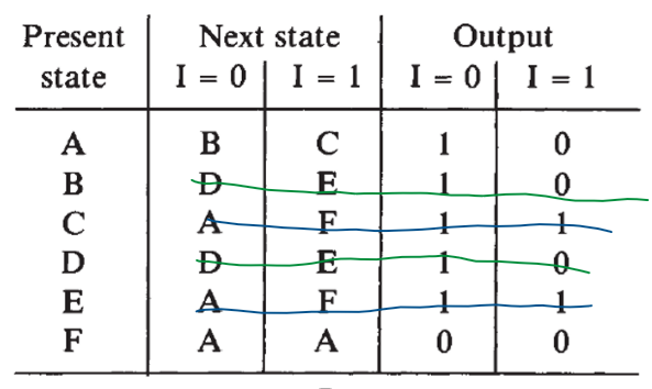
In above P/N table, \(C=E\) and \(B=D\), thus, the table can be reduced as:

Further, it can be found that \(A=B\):

A and B have been shown to be equivalent they do not lead to the same immediate next states.
The final state of the machine will however be the same regardless whether one starts from state A or state B.