9. 逻辑门实现[英]
本文最后更新于 2025年6月4日 晚上
Logic Gate Characteristics
The Tristate Gate
Tristate gate, has three output states.
- An additional control input.
- The control input is at logical 1 the gate behaves as an ordinary logic gate.
- A logical 0 on the control the gate is disabled and the output enters its third state, having a high impedance between the earth and power supply rails.
In the third state:
- The gate can only supply or sink a few microamps of current
- The gate can neither drive nor load any device connected to it
- The gate is effectively disconnected from the circuit
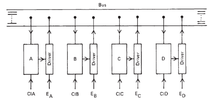
Bus(总线)
It can provide the communication from all the registers, it can transfer not a signal bit data.
The Driver of Bus can control where the data will be transferred(to the driver of register whose value of 1) A pulse is applied to the clock of the register into which the data is to be written.
Logic Families
Bipolar and Metal oxide semiconductor.
Both rely on the switching of transistors between discrete states and are suited to integrated circuit manufacture.
Bipolar Transistor
The earliest electronic logic based on diodes, cannot present NOT operation.
The voltages representing the logical constants 0 and 1m could overlap and the system fail.
Transistor can act as a two-state switch, its amplifier with 180 degree phase change.
Transistor Transistor Logic(TTL)
A multiple emitter input transistor that:
- High speed TTL has faster switching but high expense of power consumption.
- Low power TTL has lower switching and expense of power consumption.
The supply rail must be 5V for TTL.
Unipolar Logic Families
Based on the field effect transistor which requires a metal electrode separated form a semiconductor channel by an oxide insulating layer.
MOS logic devices do not require internal resistors on the chips which brings high density package.
MOS has a huge time consumption.
P-MOS
Semiconductor is p-doped, is suited to large scale integration and has a greater packing density capability than bipolar transistor.
N-MOS
N-MOS loigc is suited to large scale integration and has a greater packing density capability than bipolar transistor logic.
The circuit carriers in N-MOS are free electrons, which are more mobile than larger positive charges, and this results in faster switching times compared with P-MOS.
CMOS
Complementary metal oxide semiconductor, is faster than P-MOS, N-MOS, and is less power consumption than Low power TTL, and have a good operating time.
In alongside TTL CMOS adopts to 5V, work alone– 3V to 20V.
CMOS Circuit Logic
Fan-out
Number of logic inputs that can be driven from the output of a logic.
A typical fan-out for a TTL is 10.
With CMOS, it will drive more than 10 gates and potentially infinite.
Fan-out should be limited to 50, due to the capacitive loading of inputs.
Fan-in
The number of logic outputs that can be connected to a logic gate input.
In TTL outputs, the internal transistors will be overloaded if the outputs are connected together.
Rise Time and Fall Time
The time which taken for the lowest value to highest value, is measured from 10% to 90%.
Fall time is inversed and measured fully.
CMOS and TTL
A system may contain both CMOS and TTL.
A high output from a CMOS can drive a TTL input but if CMOS TTL’s low output can drive CMOS because the low input of CMOS is (0-1.5V).
The high output for TTL is about 3.6V, just for the high input for CMOS is (3.5-5.0V).